

Impact of Signal Loss on an RF Board
The performance of an RF board depends on its ability to carry a signal with minimal loss and distortion. Several factors can affect this performance, including impedance mismatch, crosstalk, and signal attenuation. In addition, high-frequency signals generate heat that can damage components and shorten their lifespan if not managed properly. This is why thermal management is a key aspect of any RF PCB design. In order to address this issue, designers use heat sinks and thermal vias to dissipate the heat and keep the circuit cool.
Another important factor in rf board design is the impedance matching of transmission lines. Using microstrip or stripline transmission lines with appropriate impedance values and tolerances helps ensure that the traces maintain their characteristic impedance (Z0) and avoid power losses from reflections. In addition, the geometry and layout of RF traces also impacts impedance matching, with wider trace widths and larger bend radii typically used for high-frequency applications.
Other issues that can impact signal integrity include parasitic inductance and capacitance, which can add delay or other unwanted effects to the signal. These can be minimized by keeping RF traces as short as possible and routing them away from high-speed digital traces, power planes, and other noise sources. It is also essential to reduce vias in the traces, as well as route them around critical components to minimize stray currents. Finally, a solid ground plane is essential to protect the circuit from electromagnetic interference (EMI), which can disrupt the transmission of the signal.
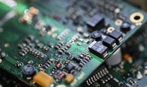
What is the Impact of Signal Loss on an RF Board?
Choosing the right materials for an RF circuit board is a crucial step in the design process. Standard materials like FR-4 work well for low-frequency PCBs, but they can suffer from high-frequency loss and other problems when used in demanding RF circuits. Choosing an alternative material such as Rogers’ ceramic or high-performance FR-4 can provide lower loss and higher stability, making it the best choice for high-frequency applications.
RF PCBs require special considerations for their layout and layout. Due to the high-frequency nature of these signals, they are more susceptible to interference from other parts of the circuit board or the surrounding environment. In order to minimize interference, it is important to use a shielding technique, such as a Faraday cage made of conductive or magnetic material, and to shield any cables that carry analog or digital signals.
Additionally, the distances over which the signals are transmitted, coupled with the need for high bandwidth and low signal loss, make RF boards indispensable in these systems. Their design must support long-distance communication, often requiring the integration of high-power amplifiers and low-noise components to ensure clear signal reception and transmission.
As technology continues to evolve, RF PCB designs are becoming increasingly compact and efficient. This is being driven by the need to reduce component size and cost, as well as the desire to increase functionality in a limited space. One trend is to integrate passive and active components directly onto the board itself, reducing the number of interconnects needed. This can help to improve circuit performance, as well as reduce manufacturing costs by reducing the amount of soldering required.