

Layer configurations for HDI boards
If you’re working with high-speed signals and fine pitch BGA components, then it’s likely that you’ll have to use HDI layout and routing techniques. This is because these technologies are the only way to guarantee that you’ll be able to work with these types of component densities without having to sacrifice performance or creating unnecessarily large PCBs.
While traditional PCBs utilize Plated Through Hole (PTH) technology that involves drilling holes through the entire board, HDI uses smaller vias like microvias, blind/buried vias and staggered vias that connect layers together in a more efficient manner. This helps reduce noise and improve signal timing, thereby increasing performance on the device.
The layer configurations for HDI boards can vary widely depending on the requirements of the design. However, there are some standard layer configurations that can be used for most applications. One of these is the 2+N+2 configuration, which consists of two sequential build-up layers that add four copper layers to the base/core/first laminations. The 2+N+2 structure is a popular choice for supporting routing into moderate pin count, high-density BGA components.
Another popular configuration for hdi board is the 1+N+1 configuration, which consists of a single signal layer sandwiched between two insulating layers with additional layers on either side. These additional layers can be ground or power planes, and they help to reduce electromagnetic interference (EMI) and improve signal integrity.
Both these configurations require a higher layer count than non-HDI boards, but they also offer greater flexibility and improved performance. Additionally, these configurations allow for more space for power and ground connections, which can be useful for high-density applications.
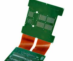
What are the typical layer configurations for HDI boards?
Another benefit of these configurations is that they make it easier to route impedance controlled traces, which can improve the performance of high-speed signals. However, it’s important to note that the high-density of these configurations can cause the board to generate more heat, so it’s essential to have a good thermal management plan in place.
Finally, it’s worth mentioning that the material selection for any HDI design is critical to ensure that it will be manufacturable. This is because the conductive and dielectric materials used in these designs can significantly influence both manufacturability and field performance. For example, some conductive materials may have an undesirable impact on the conductivity of the circuit board, while others can make it difficult to perform the soldering steps necessary to attach the components. It’s therefore recommended that designers always check their fabricator’s capabilities before committing to an HDI layout. This can help avoid creating a layout that cannot be fabricated and save significant time and money.
Microvias are drilled into the HDI board to connect different layers. Specialized laser drilling or mechanical drilling techniques are used to create these tiny vias. The drilling process requires precision to ensure that the vias are the correct size and align perfectly with the other layers. After drilling, the microvias and traces are plated with copper to create the conductive pathways. Plating involves the deposition of a thin layer of copper over the drilled vias and traces, ensuring that the electrical connections are solid and reliable.


