PCB Fabrication Assembly
Printed Circuit Board (PCB) fabrication assembly is a critical process in the electronics manufacturing industry, bridging the gap between design and functional electronic devices. This intricate process involves the creation of PCBs, followed by the assembly of electronic components to produce fully operational circuit boards. The growing demand for smaller, faster, and more reliable devices has made PCB fabrication assembly an indispensable part of technological innovation.
The process begins with PCB fabrication, which involves designing and creating the physical structure of the board. Engineers use specialized software to design the circuit layout, ensuring optimal placement of traces, pads, and vias. The design is then transferred to a substrate, typically made of fiberglass-reinforced epoxy resin. Layers of conductive materials like copper are added and etched to create the circuit paths. Additional layers are stacked and laminated to produce multi-layered PCBs for complex applications. Advanced techniques such as laser drilling are often employed to create precise vias for inter-layer connectivity.
Once the bare PCB is fabricated, the pcb fabrication assembly phase begins. This involves mounting electronic components such as resistors, capacitors, diodes, and integrated circuits onto the board. Surface Mount Technology (SMT) is the most common assembly method, where components are directly soldered onto the board’s surface. SMT offers several advantages, including compact design, faster production, and better electrical performance. For specific applications, Through-Hole Technology (THT) is used, which involves inserting component leads into drilled holes and soldering them from the other side of the board.
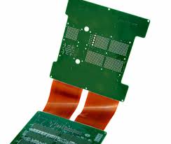
PCB Fabrication Assembly: A Comprehensive Overview
The assembly process typically starts with applying solder paste to the board’s pads using a stencil. Components are then placed on the board using automated pick-and-place machines. Once all components are in place, the board is subjected to reflow soldering, where it is heated in a controlled environment to melt the solder paste, creating solid electrical connections. For boards with THT components, wave soldering or manual soldering techniques are applied to secure these components.
Quality assurance is a critical aspect of PCB fabrication assembly. Assembled boards undergo thorough testing to ensure they meet design specifications and function as intended. Inspection methods include Automated Optical Inspection (AOI), X-ray inspection, and in-circuit testing (ICT). These tests identify issues like soldering defects, misaligned components, and open circuits. Ensuring high quality is especially important for applications in industries such as aerospace, medical devices, and automotive, where reliability is paramount.
PCB fabrication assembly has evolved significantly over the years, driven by advancements in technology. Innovations like flexible PCBs, high-density interconnect (HDI) designs, and embedded components have expanded the possibilities for electronics design. Moreover, environmental considerations have led to the adoption of lead-free solder and other eco-friendly practices in PCB manufacturing.
In conclusion, PCB fabrication assembly is the backbone of modern electronics, enabling the creation of devices that power our daily lives. From smartphones and computers to medical equipment and industrial machinery, the importance of this process cannot be overstated. As technology continues to advance, PCB fabrication assembly will remain at the forefront of innovation, paving the way for smarter, more efficient electronic solutions.