

How Does Flex PCB Fabrication Contribute to Smaller Device Designs?
As electronic devices become more advanced, there is an increasing demand for smaller, lighter, and more efficient designs. From medical wearables and smartphones to IoT devices and automotive electronics, the need for compact circuit boards is at the forefront of modern technology. Flex PCB fabrication plays a critical role in meeting this demand, offering significant advantages in reducing the size of devices while maintaining or even enhancing their performance. This article explores how flex PCB fabrication contributes to smaller device designs, allowing for more efficient use of space and improved functionality.
Compact Design Capabilities of Flex PCBs
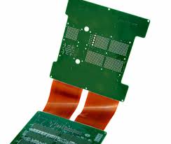
One of the most significant advantages of flex pcb fabrication is its ability to create compact circuit boards that can fit into tight spaces. Unlike traditional rigid PCBs, which are limited in their design flexibility, flexible PCBs can bend, twist, and fold without compromising their functionality. This ability allows engineers to design smaller, more compact devices by utilizing the full available space, creating a more efficient overall product.
In many applications, especially in medical devices like wearable ECG monitors or fitness trackers, space is at a premium. Flex PCBs allow for complex circuit designs that would otherwise be too large for a traditional rigid PCB. The flexibility of these boards means they can be integrated into the form factor of the device, rather than taking up additional space, which is crucial in devices that need to be both small and lightweight.
Space Efficiency Through Flexible Layers
Flex PCB fabrication also allows for the integration of multiple layers in a compact form factor. In traditional rigid PCBs, each layer is typically stacked on top of another, requiring additional space for connectors and other components. However, with flexible PCBs, manufacturers can stack the layers in a much more efficient manner, allowing for a denser and more compact circuit design.
Multi-layer flex PCBs enable the incorporation of complex circuitry and interconnections within a smaller physical area, reducing the need for external connectors and components. The ability to build complex circuit boards in a smaller space is particularly valuable for devices that require a lot of functionality in a compact form, such as smartphones and wearable health devices.
Reduced Component Size and Weight
Flex PCB fabrication can also contribute to reducing the size and weight of electronic devices by eliminating the need for additional components, such as connectors and interconnects, that are commonly required in traditional rigid PCBs. In a flex PCB design, components can be mounted directly onto the flexible circuit itself, which reduces the overall footprint of the device. The absence of bulky connectors and the ability to route the circuits in a more efficient way allows manufacturers to create lighter devices without sacrificing functionality.
Additionally, the thin profile of flexible PCBs allows for designs that are both lightweight and durable. This is particularly important in wearable devices, where comfort and portability are key considerations. With flex PCB fabrication, engineers can design thinner, more streamlined devices that are easier for consumers to wear and use without feeling weighed down.
Design Flexibility for Innovative Form Factors
One of the most innovative aspects of flex PCB fabrication is its ability to conform to non-traditional form factors. While rigid PCBs are typically confined to flat, rectangular shapes, flexible PCBs can be molded to fit into curved or uniquely shaped enclosures. This flexibility allows designers to push the boundaries of device design, creating products with shapes and configurations that were previously impossible or impractical with rigid PCBs.
For example, in medical devices such as flexible sensors or implantable devices, the ability to design PCBs that fit the natural shape of the human body is a significant advantage. Similarly, in consumer electronics like foldable smartphones, flex PCBs enable the creation of flexible, foldable designs that were once thought to be unfeasible.
Streamlined Manufacturing and Integration
Flex PCB fabrication contributes to smaller device designs not only through the physical dimensions of the boards themselves but also by streamlining the manufacturing process. The integration of flexible circuits reduces the need for multiple components, connectors, and assembly steps. By consolidating complex circuits into a single, flexible component, manufacturers can reduce the overall size of the device and eliminate unnecessary bulk, leading to a more compact and efficient product.
In many cases, flex PCBs can replace multiple rigid PCBs, which would otherwise require multiple interconnections and wiring. This reduction in the number of components and connections simplifies the overall design and manufacturing process, further contributing to the creation of smaller, more efficient devices.
Conclusion
Flex PCB fabrication plays an essential role in enabling the design of smaller, more compact electronic devices. Through its ability to bend, fold, and conform to unique shapes, flex PCBs offer unmatched flexibility in design. This capability, combined with the ability to integrate multiple layers, reduce component size, and eliminate the need for bulky connectors, allows engineers to create highly functional yet space-efficient devices. As technology continues to advance, flex PCBs will remain a critical tool for pushing the boundaries of miniaturization, making them an indispensable element in the development of smaller, more powerful electronic products.