
Blind Vias
When designing a circuit board, it is sometimes necessary to connect layers of the board with conductive holes. These holes, known as vias, can be created in multiple ways, including through hole, blind, and buried. Each type of via has its advantages and disadvantages, but using them properly can help improve the quality of a circuit board design and increase connection density. In this blog post, we will explore the main advantages of using blind vias and discuss how to use them correctly to get the best results.
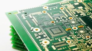
A blind via is a cylindrical conductive hole that connects the copper in one layer to the copper in another without passing through any other layers. This allows designers to reduce the number of layers required on a PCB, which is particularly useful for high-density circuit boards like those used in smartphones and laptops. Blind vias are typically fabricated using laser drilling, which allows the drill to precisely ablate the surface of the copper only to the extent needed to make the connection.
There are a few different reasons to use blind vias, the most important of which is reducing the overall layer count. As mentioned above, the use of blind via can allow you to fit more components on a smaller PCB, which can lead to better performance and lower costs. In addition, blind vias can also help to reduce signal delays by reducing the amount of time that signals have to travel through the PCB.
Advantages and Disadvantages of Blind Vias
The other reason to use blind vias is that they can be plated with copper, which can make the connections more reliable than through-hole vias. Through-hole vias can be prone to corrosion, especially when exposed to humidity or vibration. However, blind vias can be plated with copper to protect them from damage, which makes them a good option for applications that require high reliability.
The biggest downside of using blind vias is that they can be expensive. This is because the process of creating them can be time-consuming and labor intensive. This can add up when you need to create many of them. Additionally, the use of blind vias can result in signal loss or distortion if they are not designed and incorporated properly into a PCB design.
To avoid these problems, it is recommended that you always consult with a PCB designer before using blind vias in your designs. They will be able to advise you of the correct design practices and fabrication steps that need to be taken to ensure that your blind vias are reliable. They can also provide you with an estimate of the cost of creating your boards. This will give you an idea of whether or not they are worth the investment. To learn more about how we can help you with your PCB design, contact us today! Our team of experienced engineers would be happy to answer any questions you may have.